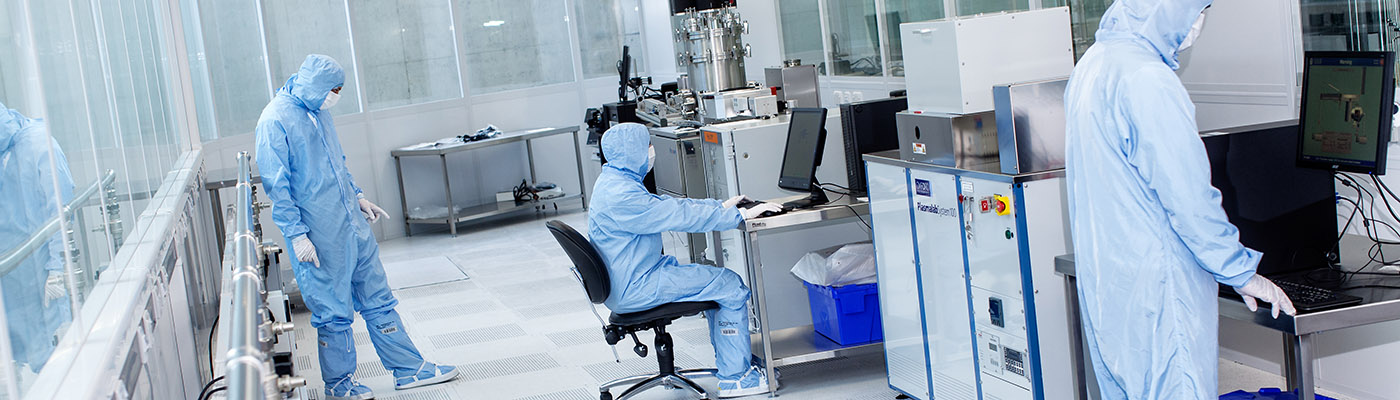
Cleanrooms
Our unique cleanroom facilities enable advanced development of 2D material capability in highly controlled environments.
The National Graphene Institute has 1500m2 of ISO class 5 & 6 cleanrooms over two floors. The nanofabrication facility is a diverse facility dedicated to 2D materials research and the production of ‘novel’ devices exploiting the properties of graphene and other 2D materials.
We have graphene layer preparation areas for atomic array extraction/alignment, inert environmental processing and UHV processing, plus an extensive range of support for nanofabrication processes as detailed below.
The cleanroom facility has extensive ‘thin film’ characterisation tools, including high resolution SEM, HRFIB, modelling Ellipsometry, Raman, large area Atomic Force Microscopy, UHV scanning probe miscopy, optical spectroscopy and profile with stress measurement.
We work in collaboration with numerous external research organisations, industry partners and SMEs in the UK, Europe and throughout the world.
2D material handling prep
Our bespoke flake transfer rigs can be used to position and transfer 2D flakes onto substrates or onto other flakes to allow the building of 2D heterostructures. Browse the links below for technical specifications:
Characterisation
You can find detail overviews and technical specifications of our characterisation equipment and capabilities by downloading the documents below:
Deposition
Plasma enhanced chemical vapour deposition (PECVD) and Inductivity coupled plasma - plasma enhanced chemical vapour deposition (ICP PECVD) are techniques that can be used to deposit a variety materials through creating a mix of reactive radicals and ions from gaseous precursors which react on the surface of the substrate to form a thin film.
You can find more detail and specifications of our CVD equipment and capabilities by downloading the documents below:
Electron beam lithography
The EBL suite has many E-beam systems: High Energy (100kv), SEM EBL, large area (200mm), & dual beam (Ion & EBL). Supports processes such as resist (+ve & -ve) spinning and supports deposition and etching.
The High Energy Raith EBPG5200 is a dedicated system designed specifically for EBL with electron beam energy up to 100kV. The use of 100kV ensures that backscattered electrons remain mostly in the substrate and that the forwarding scattering angle is small, allowing for very narrow lines and dense arrays especially since proximity effects are also small at a high beam energy. Line widths down to 6nm are possible with this tool.
Other advantages with 100kV include a small spot size of <20nm even at a high beam current of 20nA as well as a high throughput which allows large area exposures such as a full 8-inch wafer or 6-inch photomask plate.
This EBL tool is available for collaborative work with academic as well as commercial clients and is critical for the fabrication of a wide variety of nanoscale devices on various substrates.
Read a detailed overview and technical specifications of our EBL capability by downloading the documents below:
Etching
Inductively coupled plasma reactive ion etching (ICP RIE) is a technique that can be used to etch a variety of materials through creating a mix of reactive radicals and ions from gaseous precursors. These react on the surface of the substrate to selectively etch target materials.
Read detailed overviews and technical specifications of our etching capabilities below:
Photolithography
Photolithography is one of the key techniques used in the manufacture of prototype electronic devices at the NGI which allow the analysis of the electronic properties of 2D materials.
In order to describe the photolithography process, it is useful draw on its similarities with photography. In both processes an image or pattern is transferred onto a substrate by exposing a thin film of material to radiation in the visible to ultra-violet range.
The regions exposed to radiation undergo a chemical reaction, which is subsequently enhanced and further processed by the application of heat and the interaction with other chemicals. The pattern on this thin film of photoresist is thus “developed”, which in lithography involves leaving a pattern of resist on the substrate, which may represent the direct image of the intended structure or its negative image.
Find out more about our specific capabilities via the links below:
Wet chemistry
The NGI cleanroom has a large wet chemistry area, making it possible for the research of graphene and other 2D materials to incorporate a selection of methodologies. These techniques enable device fabrication to include such things as metal etches, anisotropic silicon etches, and chemical cleaning. Find out more: